
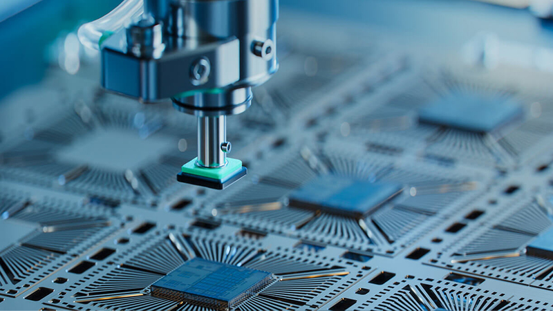
COSEN is deeply engaged in the semiconductor industry, covering silicon wafer CMP process supporting equipment and high-precision testing solutions.Relying on machine vision and precision motion control technology, wafer surface defect detection and process parameter monitoring are realized to help improve yield and production efficiency.
COSEN is deeply engaged in the semiconductor industry, covering silicon wafer CMP process supporting equipment and high-precision testing solutions.Relying on machine vision and precision motion control technology, wafer surface defect detection and process parameter monitoring are realized to help improve yield and production efficiency.
Silicon wafer CMP processes demand nanometer-level motion stability and real-time surface monitoring, yet conventional equipment lacks integrated precision motion control and machine vision feedback, leading to thickness non-uniformity and undetected surface damage.
As semiconductor nodes advance below 10nm, wafer surface defects become increasingly microscopic and complex, exceeding the detection limits of conventional optical systems that lack the advanced vision algorithms and high-resolution optical-electrical integration required.
CMP equipment generates vast process data, but without integrated industrial IoT and big data analytics platforms, manufacturers cannot correlate process parameters with defect patterns, missing opportunities for intelligent process optimization and predictive maintenance.
PREV
NEXT
The assembly line has a built-in deep learning vision system, which captures defects such as PIN offset, warped feet, missed insertion, and virtual welding in real time, distinguishes between subtle process deviations and real defects, and the detection speed is not reduced by the addition of AI.
Traditional defect classification relies on manual re-judgment.The AI audit system of the PIN intelligent assembly line can automatically learn and adapt, quickly classify and grade defects, reduce misjudgment without slowing down the production line.
The assembly line integrates a high-precision measurement module to accurately measure PIN height, coplanarity, spacing and solder joint morphology.AI-driven contour modeling improves measurement accuracy and reliability, and helps manufacturers control process fluctuations.
AI fully interconnects the various stations, testing equipment and MES systems of the assembly line, drives cross-system data fusion and analysis, and generates real-time process response prediction, dynamic beat optimization, and intelligent production scheduling.
PREV
NEXT
The massive amount of data in the manufacturing process is analyzed in real time through the AI system to gain insight into trend deviations and abnormal patterns, provide full-link traceability, and promote continuous improvement and yield improvement.
AI migrates image processing and data computing to edge GPUs, reducing the hardware cost of traditional industrial computers, while improving computing power density and response speed.
The global service team uses AI predictive maintenance to identify equipment abnormalities in advance and provide customers with faster remote diagnosis and on-site support.
From process programming to daily operation and maintenance, AI automates and optimizes processes in all aspects to improve the efficiency and production capacity of engineers and operators.
PREV
NEXT
The assembly line has a built-in deep learning vision system, which captures defects such as PIN offset, warped feet, missed insertion, and virtual welding in real time, distinguishes between subtle process deviations and real defects, and the detection speed is not reduced by the addition of AI.
Traditional defect classification relies on manual re-judgment.The AI audit system of the PIN intelligent assembly line can automatically learn and adapt, quickly classify and grade defects, reduce misjudgment without slowing down the production line.
The assembly line integrates a high-precision measurement module to accurately measure PIN height, coplanarity, spacing and solder joint morphology.AI-driven contour modeling improves measurement accuracy and reliability, and helps manufacturers control process fluctuations.
AI fully interconnects the various stations, testing equipment and MES systems of the assembly line, drives cross-system data fusion and analysis, and generates real-time process response prediction, dynamic beat optimization, and intelligent production scheduling.
The massive amount of data in the manufacturing process is analyzed in real time through the AI system to gain insight into trend deviations and abnormal patterns, provide full-link traceability, and promote continuous improvement and yield improvement.
AI migrates image processing and data computing to edge GPUs, reducing the hardware cost of traditional industrial computers, while improving computing power density and response speed.
The global service team uses AI predictive maintenance to identify equipment abnormalities in advance and provide customers with faster remote diagnosis and on-site support.
From process programming to daily operation and maintenance, AI automates and optimizes processes in all aspects to improve the efficiency and production capacity of engineers and operators.

 中文
中文
 English


